Design recommendations to optimize PCB production costs
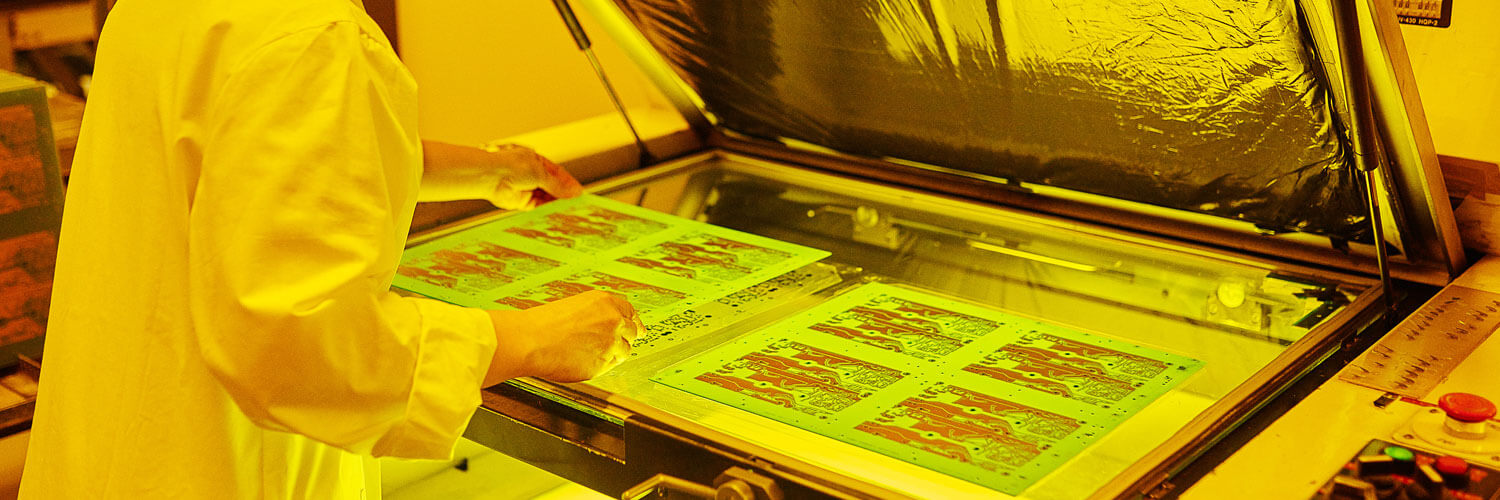
1. Preparation of PCB design for production – panelization and mechanical process
Printed circuit boards can be supplied as single pieces or in panels. Making tiles in panels is an economic solution.
The dimensions of the panels (or individual PCBs) can be milled or V-cut (scored). The standard milling tolerance is +/- 0.2 mm. In the case of scoring, the dimensions of PCBs can be increased by approx. 0.4 mm. When designing PCBs, one should take into account what degree of accuracy of machining dimensions is actually necessary.
A typical cutter has a diameter of Ø = 2 mm.
The printed circuit boards should, if possible, be blocked so that it is possible to use a tool with this diameter. “Milling finishing” must be avoided; always plan connecting elements that will keep individual tiles in the panel.
Certain sizes of technological forms must be entered into the production lines, which are multiples of panels’ sizes. It’s best to avoid square panels – it is more difficult with them to obtain the optimal cut from a laminate board.
2. PCB mosaic shape and symmetry of copper areas
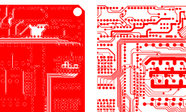
Our observations support the conclusion that the more empty spaces there are in the PCB area, the more copper is deposited on the mosaic during galvanisation, with individual tracks or pads being particularly favoured. This means that if in the area of one PCB layer there are both mass pads and loosely spaced tracks and solder pads, the thickness of the copper that will settle on loosely spaced mosaic elements will be much higher than in the mass areas. Such a distribution of copper significantly impedes further PCB manufacturing processes, and some of them need to be repeated several times.
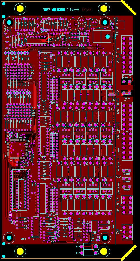
A similar problem is created by PCBs where one layer is practically a mass, and the other is a mosaic, which is characterized by so-called lack of copper surface symmetry between the Top and Bottom sides.
In the example shown: TOP (Cu: 19572 mm²) and BOTTOM (Cu: 6677 mm²).
In this situation, it is advisable to make corrections to the PCB design, whose main purpose should be to eliminate the difference in the copper surface between the TOP and BOTTOM layers.
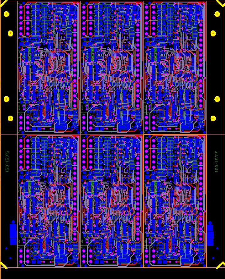
A lack of copper symmetry between the TOP and BOTTOM sides can be eliminated by proper preparation of the panels; it is possible to use technological areas of the panel for this, i.e. frames separating a single PCB.
The introduction by the designer of additional copper pads in the area of the frames would improve its symmetry. Eliminating a lack of symmetry is possible at the level of blocking the panels on the technological form, nevertheless, it leads to an increase in laminate costs by about 20% and extending the workload of various technological operations, which results in an additional increase in the PCB production costs.
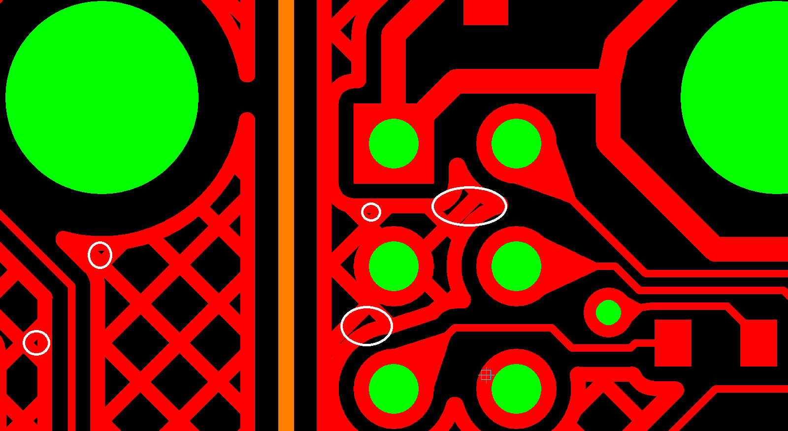
3. Track width and track spacing
The recommended minimum track width and track spacing is > 0.2 mm.
Pay attention to the actual need to enter tracks / spacings ≤ 0.2 mm. The number of such places in the mosaic should be limited to the minimum necessary.


It should be remembered that the higher the thickness of the base copper on the laminate, the greater the loss in width of the tracks in the PCB manufacturing process; therefore, for PCB designs in which there are tracks with widths ≤ 0.2 mm, laminate 18/18 μm Cu or 18/0 μm Cu should be used.
One should avoid small elements in the mosaic as well as in inscriptions and symbols designed in copper.
4. Additional remarks
- Typical colours of the solder mask (green) and description of elements (white) should be used
- Do not apply peelable masks to holes with diameters > 2 mm
- For each new order (also new version), mechanical process drawings must be generated and sent
- The PCB manufacturing technology should not be made more complicated if the product does not require it.